 Japanese
Integrated Electronic CADCSiEDA
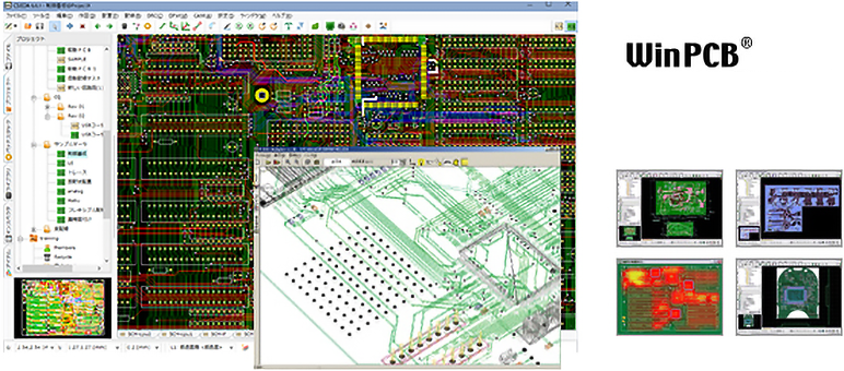
WinPCB
PRINTED CIRCUIT BOARD DESIGN TOOL
Our tool features a wide range of capabilities to support the design of everything
from analog/power/flexible circuit boards to multilayer circuit boards.
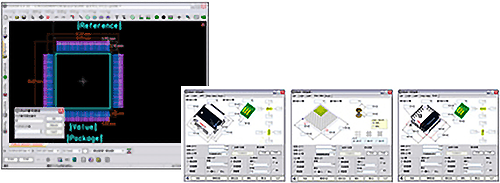
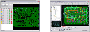
[Parts] Automatic generation of symbol shapes
Package builder
Easily create symbol shapes for DIP, SOP, QEP, BGA, and PLCC by simply entering numerical values, eliminating the need for complicated symbol creation.
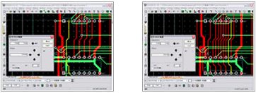
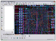
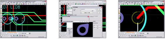
[Wirings] A variety of wiring functions.
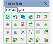
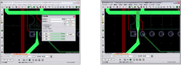
Shape processing box
"Minimize the number of clicks" and "simplify complex processes".
Based on feedback from designers, we have incorporated shape processing box functionality to support these requests.
By simply clicking on various icons, users can execute a wide range of functions, resulting in a further reduction in design time.
Wiring alignment pitch adjustment function
First click: Select the wire you want to shield.
Second click: Select the [Wire Shield] button.
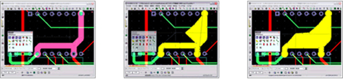
Copper pour feature
First click: Select the wire you want to create a copper pour for.
Second click: Click the "copper pour" button.
Third click: You can now freely modify the copper pour.
Wiring Alignment Pitch Function
First click: Select the wire to be aligned.
Second click: Select the [Align Pitch] button and enter the desired pitch to be changed.
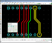
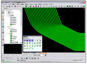
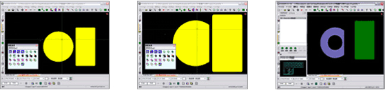
Parallel wiring function
First click: Select the pad where you want to create parallel wiring.
Second click: Click the [Parallel wiring button] and enter the desired pitch.
* You can end parallel wiring with vias (diagonal, straight, downward, upward) while in the process.
Object snap (wire pulling-in) function
Even if the wiring and pad grids are misaligned, the wiring can be snapped to the pad.
Wiring pitch function
First click: Select "[T-branch wiring]" during wiring.
Second click: Enter the starting and ending line widths.
Offset function
First click: Select the wiring to be continuously copied.
Second click: Select the [Offset wiring] and enter the pitch and number of copies to be made.
Wire Bundle
First click: Select [Bundled wiring] .
Second click: Enter the number of wires and pitch for the wiring
* You can choose between arc mode, c-cut, and straight.
Build-up wiring
Support for various designs with build-up wiring such as motherboards.
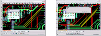
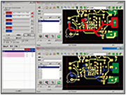
Various Functions
Copper pour feature
First click: Select the pad you want to convert to a clinch pad.
Second click: Select [Customize Pad], and enter the values.
* Supports clinch, rounded corner, breadboard, and tear drop shapes.
Custom Pad Creation Function
First click: Select the circular or square copper plane for the pad you want to create a land cut for.
Second click: Choose the [Copper Feature] option and perform a copper cut to create the desired shape.
Third click: Change the copper feature to a pad with the desired land cut shape.
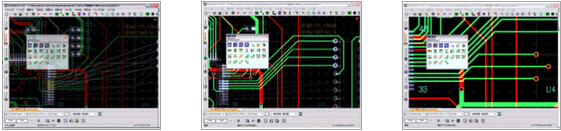
Automatic copper pour and floating copper removal function
First click: Select the copper feature where you want to remove automatic or floating copper pour.
Second click: Select the option for [automatic copper pour removal] or [floating copper removal]
Drawing creation function
Drawing creation function
You can select the area you want to zoom in on and place a magnified drawing.
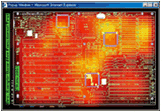
Drawing creation function
Net density information, Component density information, Component heat generation information, Wiring density information, Component height information, Component current value information, VIA density information, Component weight information.
Restoration from Gerber data
Gerber in
You can load not only data output from WinPCB but also Gerber data output from other companies.
* After importing Gerber into WinGerber, convert the data to WGG file and input it into WinPCB.
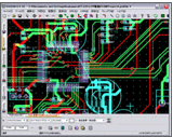
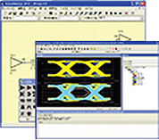
Diverse verification functions considering PCB manufacturing
 ※
※
Printed Circuit Board Design Verification Tool
Equipped with DFM/DFE verification functions. Includes DRC function and electrical characteristics check taking into account the manufacturing of printed circuit boards.
Integration with PollEx starts from CSiEDA Ver.6.
EMI/EMC measures (noise reduction measures)

EMI Suppression Design Support Tool

Signal Verification by Circuit Design
Automatic Advice System
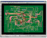
CSiEDA is an integrated electronic CAD system that supports the entire process of electronic circuit design. It is capable of total design from circuit design to PCB design/electromechanical design. We provide various simulations for high-quality PCB design in addition to shortening the design process. WinPCB offers high functionality for digital/analog design.
With the recent trend of miniaturization, high density, and high-layer PCBs, CSiEDA enables designers to achieve their intended designs with trimming, shape division, automatic placement, automatic shielding, and build-up board support. In addition, the split design function allows designers to divide design tasks and shorten delivery times. When transitioning from other CAD systems, existing design data can be utilized by converting ASC/Gerber data to WinPCB.
OVERVIEW
Menu customization
Icon customization
Macro function using Java and VB script
Backup function (file number and time settings available)
Zoom in/zoom out/fit to screen/full screen display
Zoom in/zoom out using scroll button
SQL database support
Component/drawing converter for Ver.4.0
Design in millimeters/mils
Print preview/offset function
Arbitrary movement of origin
Virtual origin
Undo/Redo (MAX=20)
DXF input/output support
Support for split design
Filter function (selectable by attribute values such as line width)
Move and arrange components with Enter key
Operation cancel and selection mode with ESC key
Expandable to 1,024 layers
Layer lock function
Conversation layer display
Pair layer display
Customizable display
Direct 3DView display
Various CAD I/F (data, drawing, netlist)
Trace function
Fill/outline display
OLE
Menu usage/unused, display/hidden settings available
Inspector function (change item properties (database))
CREATING COMPONENTS
Extension of the pad stack function (up to 1,024 layers)
Users can register their created pads in the pad stack
Support for inner layer thermal (45/90 degrees), clearance, and land creation
Automatic/manual updating of pad numbers
Functionality for creating pads using JavaScript
Component creation wizard
Offset copy/move function
Support for restricted wiring areas
Support for restricted via areas
Support for copper forbidden area
Support for component height areas
Support for copy/paste functionality
Pad rotation angle specification
Drawing rotation angle specification
Trimming
Shape division
Setting of reference name/attribute size
Double-sided reference name placement
Changing the origin position of the text size
Setting of text pitch
PCB CREATION
Moving components at the center or at pin 1
Support for moving items using the keyboard arrow keys
Alternate specification support for components on the component side/solder side
Support for moving/deleting component pads
Add Pad Functionality to Component
Add Pads
Add Test Points
Attribute changes (individual/batch)
Cutting component silk screen
Component class settings
Component mounting type settings
Component changes (individual/batch)
Offset placement
Matrix placement
Radial placement
Component locking
Component list
Editing component silk screen
PLACEMENT
Improvement of wiring editing
Wiring loop check
Wiring movement
Wiring offset movement
Wiring line exchange
Taper wiring function
Parallel wiring function
Wiring pitch width specification function
Wiring highlighting display
Angular wiring function
Wiring copy function
Wiring offset copy function
Trapezoidal wiring function
Net name ON/OFF
Pad number display ON/OFF
Wiring length setting
Tear drop wiring
Automatic wiring
Semi-automatic wiring
IVH via
Build-up board
Pad-on-via
3D realistic display design
Net addition
Net swap
Net color coding
Division of the same net
Editing net name
Net deletion (individual/batch)
Net display ON/OFF
Support for start angle specification of wiring corner (e.g., 45-degree corner starting position)
Support for 45/90-degree thermal wiring
Direct copper conversion function for wiring
BOARD OUTLINE
PCB outline creation function from DXF data
Line offset function
Rounding corners function for PCB
Auxiliary line function
Offset copy/move function
Trimming function
Command-line input (absolute/relative)
COPPER
Offset function for copper (inner/outer)
Function to combine copper shapes
Copper extraction function
Function to specify cutouts in copper shapes
Trimming of copper shapes
Editing of copper shapes
Transformation of shapes into copper (DXF/Gerber data)
Normal copper shapes
Copper cutout shapes
Auto copper shapes
Function to automatically remove floating copper shapes
PowerPlane
Internal layer division
SHAPE
Extension of trimming function
Enhancement of drawing functions (direct editing of circles and arcs)
Support for angle specification of shapes and components
Option to create auxiliary lines on a per-layer basis
Option to delete auxiliary lines as needed
Batch trimming
Alignment function
Evenly spaced arrays
Object snap
Internal layer division
DRC
Net check function
DRC inner layer check
Prohibited area for component placement
Prohibited area for vias
Prohibited area for wiring
Prohibited area for copper planes
Prohibited area for component height
Online DRC
DRC design log
Shortest distance measurement
Batch measurement of shortest distance
Wiring angle check
Measurement tool
CAM
274D/274X Gerber compatibility
NC drill output
NC coordinate/tool table separation
Excellon output
NC hole instruction diagram data
Mounting component coordinate output
Surface mounting (compatible with mixed surfaces)
Gerber-in
Board inversion
Board rotation (45, 90, 180 degrees)
Gerber data output (individual, batch)
MATERIALS
Drawing enlargement function
Wiring database report
Via list report
Wiring length report
Pad stack report
Temperature distribution map
Component placement information report
Height component diagram
Site placement distribution diagram
Density distribution map
Netlist output
Assembly drawing creation
Wiring density distribution diagram
Display of pattern outline for inspection
3D mounting diagram
CONTACT US
- +81-6-6377-2451
9:00 - 18:00 (JST) on weekdays. - INQUIRY